Ask AI
— answers from the official manualAnswers from the official manual.
Common questions
Common Questions
20 totalWhat is the input power voltage range for the reServer Industrial?
The reServer Industrial accepts DC 12V-36V input via a 2-pin terminal block connector. A 24V/5A power adapter (without power cord) is included in the package. The system has a 10A current limit, and the Power LED lights up red after plugging in the power supply. (Page 5)
How do I enter recovery mode to flash the system on the reServer Industrial?
While the board is powered up, press the RECOVERY button (SW2) to enter recovery mode, which allows you to flash the system of the core board. The recovery button is labeled FORCE_RECOVERY in the schematic. If you need to reflash the OS image, refer to the Seeed wiki for details. (Page 7)
What do the LED indicators on the reServer Industrial mean?
The Power LED is red and serves as the 3.3V power indicator, staying always on after power is applied. The Run/State LED is green and serves as the system operation indicator, staying always on or blinking after the system is running. (Page 5)
What is the maximum PoE power output supported on the 4 LAN ports?
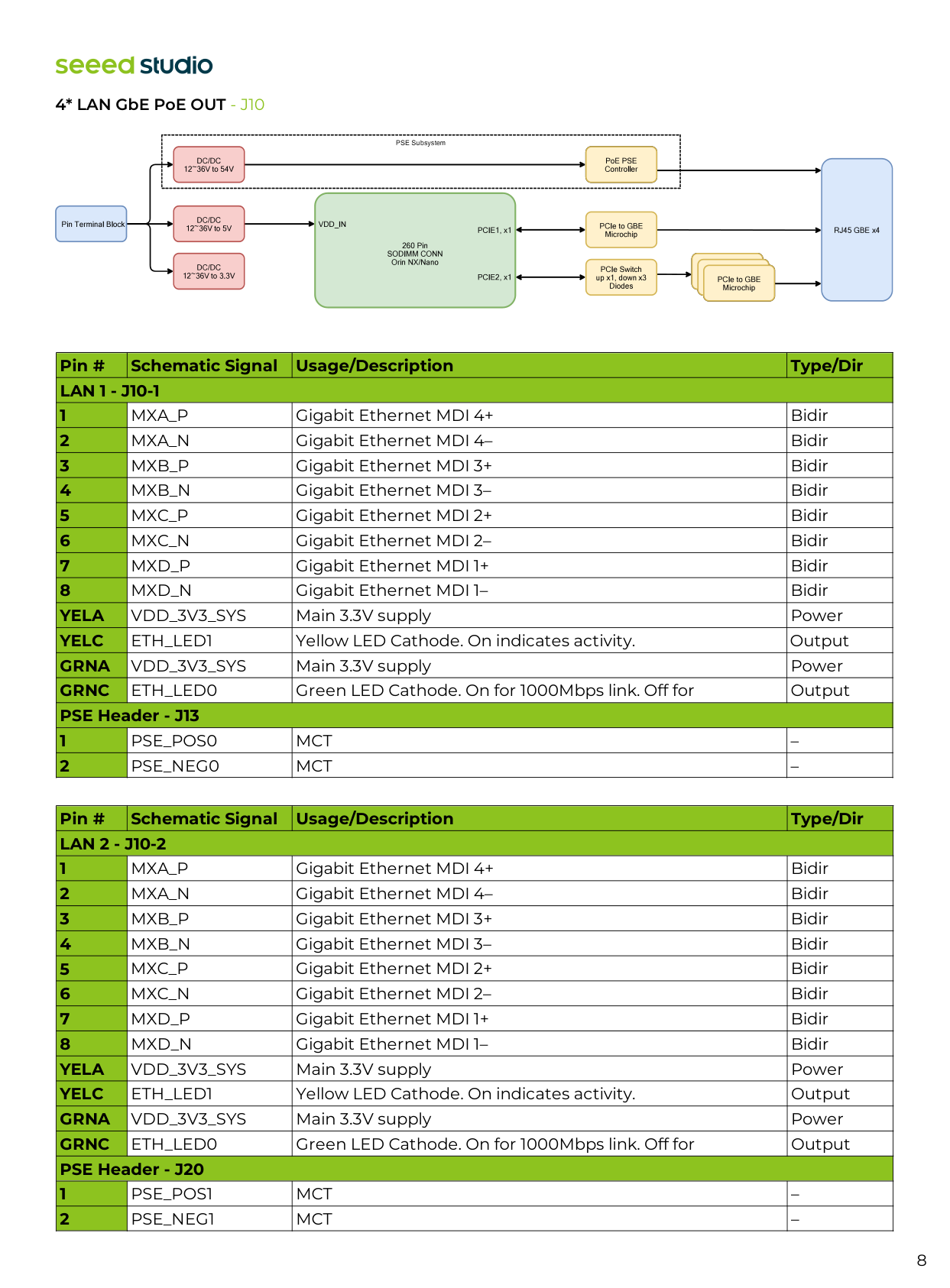
Each of the 4 PoE ports supports PSE 802.3af with up to 15W per port. With all 4 ports simultaneously connected, the total power supply capacity can reach 60W. All 4 LAN PoE ports support Gigabit Ethernet at 10/100/1000Mbps. (Page 9)
What serial communication modes does the COM port support, and how do I switch between them?
The COM port (DB9 J1) supports RS232, RS422, and RS485 modes, with the default mode being RS485. You switch modes by toggling the DIP switch (SW3), and this must be done after powering off the device to avoid damage. RS232 comes with flow control, and the full mode selection table is controlled by three switch positions (Mode_0, Mode_1, Mode_2). (Page 11-12)
What storage options are supported on the reServer Industrial?
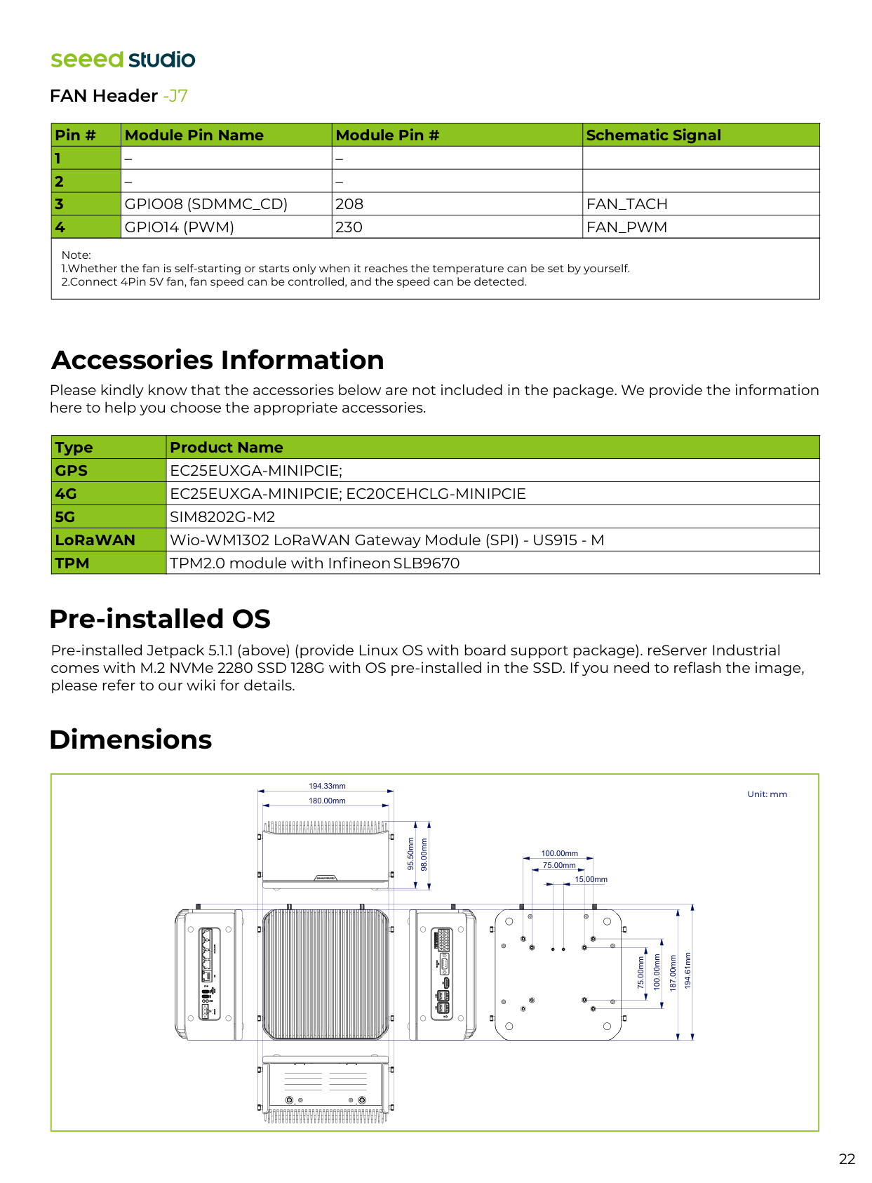
The reServer Industrial supports two 2.5" SATA HDD/SSD drive bays via SATA III at 6.0Gbps, supporting SSDs, HDDs, and 4TB HDDs up to 15mm thick. It also includes one M.2 Key M (2280) slot supporting PCIe Gen4.0 NVMe SSD, and comes with a 128GB M.2 NVMe SSD pre-installed with the OS. (Page 21-22)
Show 14 more questions
What USB ports are available on the reServer Industrial and what are their limitations?
How do I factory reset the [product]?
What is the maximum power consumption of the PoE ports?
How do I switch between RS232/RS422/RS485 modes?
What are the dimensions of the [product]?
How can I control the fan settings?
What are the operating temperature and environmental specifications for the reServer Industrial?
Can I use both the M.2 Key B slot and the Mini PCIe slot at the same time?
How do I perform a hard reset on the reServer Industrial?
What are the video encode/decode capabilities?
How do I set up the RTC backup battery?
How do I install SIM cards and use M.2 modules?
What are the storage options available?
How do I switch between USB host and debug modes on J8 header?
Full Manual
24 pages
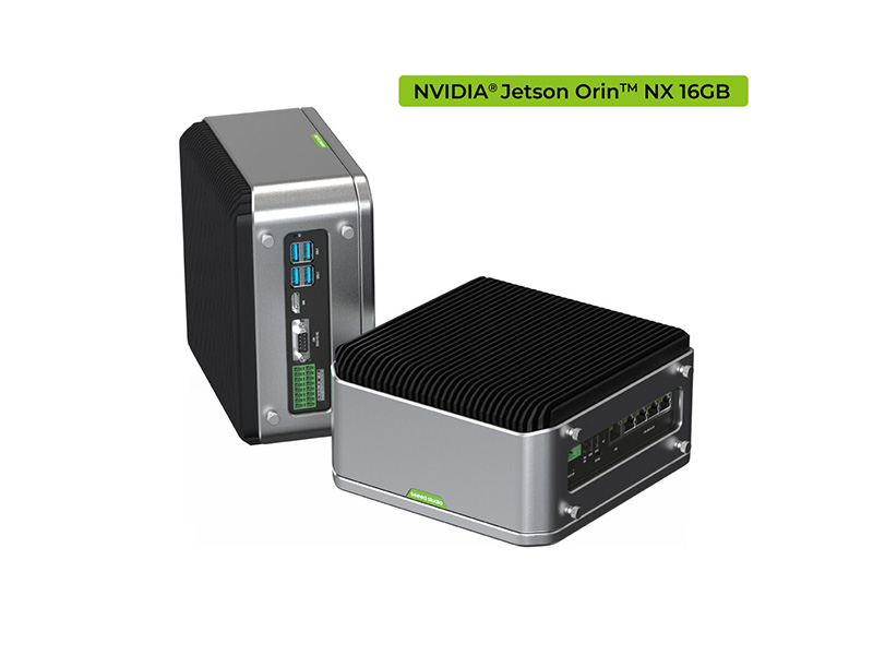
1 reServer Industrial Reference Guide 1* reServer Industrial 1* DIN Rail Bracket 10* Bracket Screw 1* 16-Pin Terminal Block for DIO 1* 24V/5A Power Adapter(without power cord) 1* 2-Pin Terminal Block Power Connector Introduction reServer Industrial-series offers fanless compact AI-enabled NVR server built with NVIDIA advanced AI embedded systems: Nvidia Jetson Orin™ NX/Orin™ Nano delivering AI performance from 20 TOPS to 100 TOPS. With pre-installed OS system, PoE interfaces, rich extension modules, industrial peripherals, Hybrid network connectivity, thermal management, expandable storage combined with decades of Seeed’s hardware expertise, reServer Industrial Jetson is ready to help you accelerate and scale the next-gen AI products emerging diverse AI scenarios. Packing List Fanless compact AI-enabled NVR server Wider temperature support -20 ~ 60°C with 0.7m/s airflow Expandable storage 2 Drive Bays to support 2.5" SATA HDD/SSD; 1* M.2 2280 M key socket for NVMe SSD Multi-stream processing 5* GbE RJ45(4 for 802.3af PSE); support multiple 4K streams with real-time processing complex tasks Hybrid connectivity Support 5G/4G/LTE/LoRaWAN® (Module optional) with 1* Nano SIM card slot Design for industrial interfaces
1* Com(Rs232/422/485); 4* Di/Do; 1* Can; 4* Usb3.1;
1* TPM2.0 (Module optional)
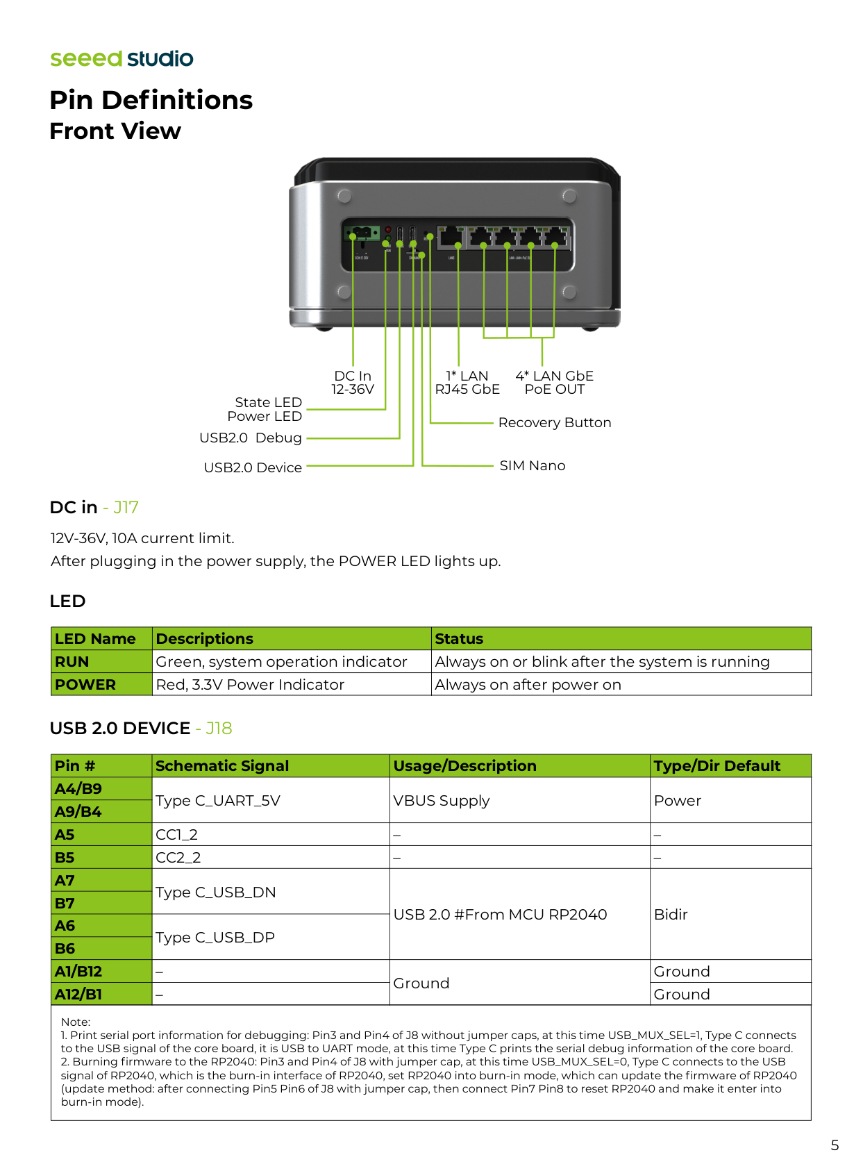
Table of Contents 2 Introduction Part list Hardware Overview Specifications Block Diagram Pin Definitions 1 1 3 3 4 5 5 5 5 5 6 6 7 7 7 9 10 10 11 12 13 14 15 15 16 17 17 17 17 17 18 18 19 19 20 21 21 21 22 22 22 22 23 24 24 Front View DC in - J17
Led
Usb 2.0Device - J18
Usb 2.0 Debug - J19
Nano SIM card slot - J6 RECOVERY Button - SW2 GbE connectorLan0 - J14
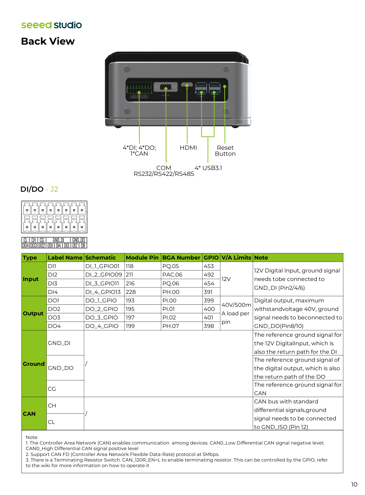
4* LAN GbE PoE OUT - J10 Back ViewDi/Do - J2
Com 232/422/485 - J1
Mode selection instructions HDMI Port - J16 USB3.1 TYPE-A x2 - J3 USB3.1 TYPE-A x2 - J4 RESET Button Carrier board Control and UART Header - J8 DIP Switches - SW3Rtc
RTC-Pin Header - J12 RTC-Coin Cell Battery Socket - J22Led
M.2 Key M - J21 TPM Header - J11 Mini PCIe - J5 M.2 Key B - J6Sata - J27, J30
SATA Data Connector SATA Power Connector - J28, 29 FAN Header -J7 Accessories Information Pre-installed OS Dimensions Flexible mounting Certifications More information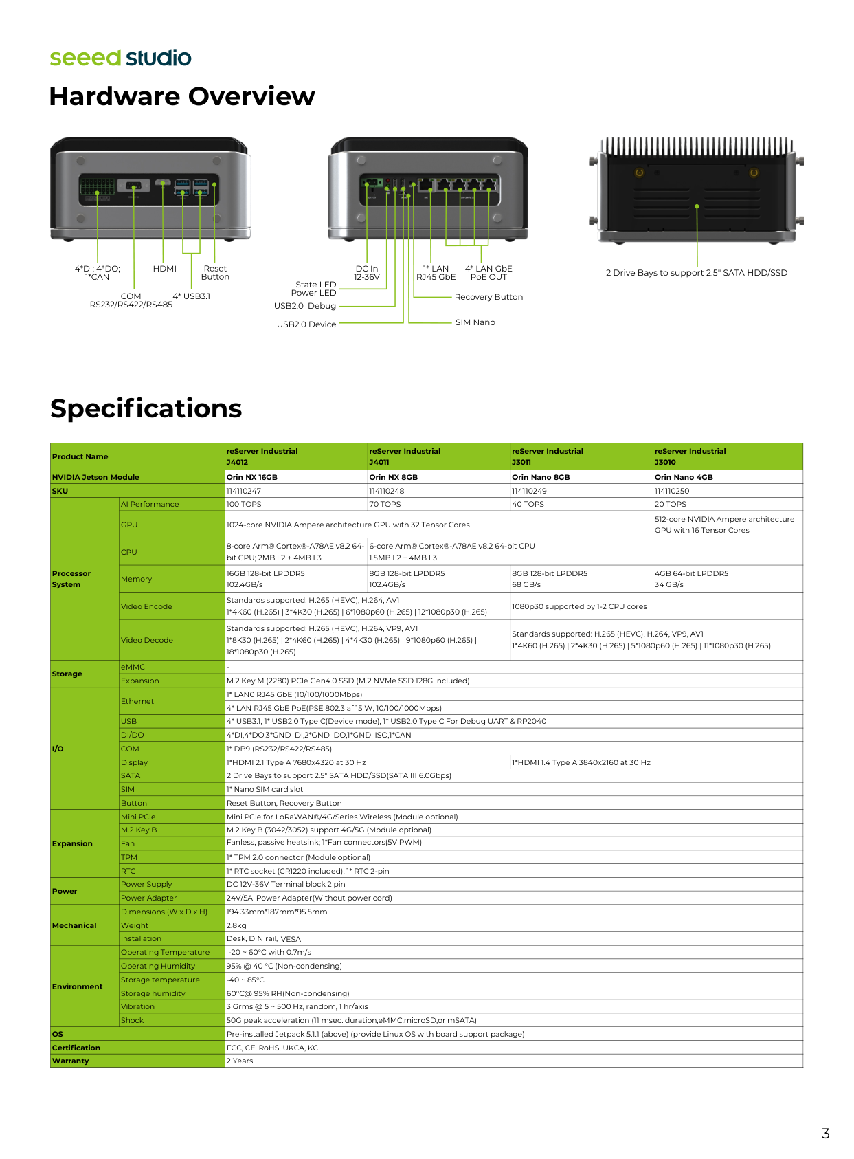
3 Hardware Overview Specifications
4*Di; 4*Do;
1*Can
Com
Rs232/Rs422/Rs485
Hdmi
4* Usb3.1
Reset Button DC In12-36V
1* Lan
RJ45 GbE 4* LAN GbE PoE OUT Recovery Button SIM Nano State LED Power LED USB2.0 Debug USB2.0 Device 2 Drive Bays to support 2.5" SATA HDD/SSD 114110247 114110248 114110249 114110250 AI Performance100 Tops
70 Tops
40 Tops
20 Tops
Gpu
1024-core NVIDIA Ampere architecture GPU with 32 Tensor Cores 512-core NVIDIA Ampere architecture GPU with 16 Tensor CoresCpu
8-core Arm® Cortex®-A78AE v8.2 64- bit CPU; 2MB L2 + 4MB L3 6-core Arm® Cortex®-A78AE v8.2 64-bit CPU1.5Mb L2 + 4Mb L3
Memory 16GB 128-bit LPDDR5 102.4GB/s 8GB 128-bit LPDDR5 102.4GB/s 8GB 128-bit LPDDR5 68 GB/s 4GB 64-bit LPDDR5 34 GB/s Video Encode Standards supported: H.265 (HEVC), H.264, AV1 1*4K60 (H.265) | 3*4K30 (H.265) | 6*1080p60 (H.265) | 12*1080p30 (H.265) 1080p30 supported by 1-2 CPU cores Video Decode Standards supported: H.265 (HEVC), H.264, VP9, AV1 1*8K30 (H.265) | 2*4K60 (H.265) | 4*4K30 (H.265) | 9*1080p60 (H.265) | 18*1080p30 (H.265) Standards supported: H.265 (HEVC), H.264, VP9, AV1 1*4K60 (H.265) | 2*4K30 (H.265) | 5*1080p60 (H.265) | 11*1080p30 (H.265) eMMCUsb
4* USB3.1, 1* USB2.0 Type C(Device mode), 1* USB2.0 Type C For Debug UART & RP2040Di/Do
4*Di,4*Do,3*Gnd_Di,2*Gnd_Do,1*Gnd_Iso,1*Can
Com
1* Db9 (Rs232/Rs422/Rs485)
Display 1*HDMI 2.1 Type A 7680x4320 2 Drive Bays to support 2.5" SATA HDD/SSD(SATA III 6.0Gbps) at 30 Hz 1*HDMI 1.4 Type A 3840x2160 at 30 HzSata
Sim
1* Nano SIM card slot Button Reset Button, Recovery Button Mini PCIe Mini PCIe for LoRaWAN®/4G/Series Wireless (Module optional) M.2 Key B M.2 Key B (3042/3052) support 4G/5G (Module optional) Fan Fanless, passive heatsink; 1*Fan connectors(5V PWM)Tpm
1* TPM 2.0 connector (Module optional)Rtc
1* RTC socket (CR1220 included), Product Name reServer IndustrialJ4012
reServer IndustrialJ4011
reServer IndustrialJ3011
reServer IndustrialJ3010
NVIDIA Jetson Module Orin NX 16GB Orin NX 8GB Orin Nano 8GB Orin Nano 4GBSku
Processor System StorageI/O
Expansion Power Mechanical EnvironmentOs
Certification Warranty 1* RTC 2-pin Power Supply DC 12V-36V Terminal block 2 pin Power Adapter24V/5A
Power
Adapter(Without
power
cord) Dimensions (W x D x H) 194.33mm*187mm*95.5mm Weight Installation Desk, DIN rail,
Vesa
Operating Temperature -20 ~ 60°C with 0.7m/s Operating Humidity 95% @ 40 °C (Non-condensing) Storage temperature-40 ~ 85°C
Storage humidity 60°C@ 95% RH(Non-condensing) Vibration 3 Grms @ 5 ~ 500 Hz, random, 1 hr/axis Shock 50G peak acceleration (11 msec. duration,eMMC,microSD,or mSATA) Pre-installed Jetpack 5.1.1 (above) (provide Linux OS with board support package) FCC, CE, RoHS, UKCA, KC 2 Years 2.8kg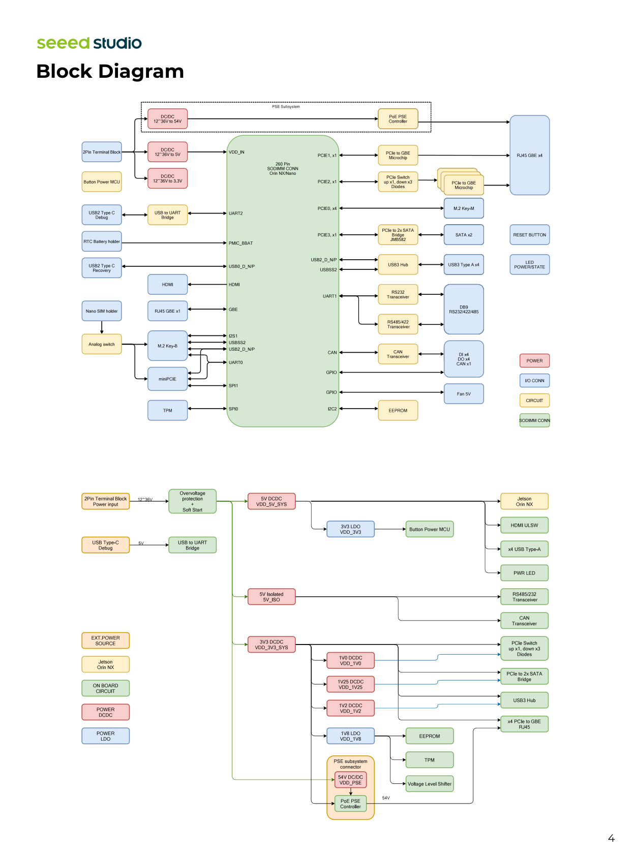
4 Block Diagram
5
Led
12V-36V, 10A current limit. After plugging in the power supply, the POWER LED lights up. Pin Definitions Front View DC In12-36V
1* Lan
RJ45 GbE 4* LAN GbE PoE OUT Recovery Button SIM Nano State LED Power LED USB2.0 Debug USB2.0 Device DC in - J17Usb 2.0 Device - J18
Note:Run
Power
Green, system operation indicator Always on or blink after the system is running Red, 3.3V Power Indicator Always on after power on Pin # Schematic Signal Usage/Description Type/Dir DefaultA4/B9
A9/B4
A5
B5
A7
B7
A6
B6
A1/B12
A12/B1
Type C_UART_5V VBUS Supply PowerCc1_2
– –Cc2_2
– – Type C_USB_DN USB 2.0 #From MCU RP2040 Bidir Type C_USB_DP – Ground Ground – Ground
6 Note: 1.The computer can recognize the board information: USB 2.0 Device interface on the core board, which can use Type C cable for data communication. 2.Burning image to Jetson: While the board is powered up, press the RECOVERY button SW2 to enter the recovery mode, which allows you to burn in the system of the core board.
Usb 2.0 Debug - J19
Note:A4/B9
A9/B4
A5
B5
A7
B7
A6
B6
A8
B8
A1/B12
A12/B1
Gpio00
(Usb_Vbus_En0)
87Usb0_Vbus_Det*
VBUS Supply Power – –Cc1_1
– – – –Cc2_1
– –Usb0_D_N
109Usb0_Ap_N
USB 2.0 #0 Data BidirUsb0_D_P
111Usb0_Ap_P
– – – – – – – – – – – – – Ground Ground – – – GroundPin
Schematic SignalPin
Schematic SignalC1
C2
C3
C4
C5
C6
C7
G1,G2,G3,G
Sim_Clk
Sim_Dio
Sim_Rst
Nc
Vdd_Sim
Gnd
Sim_Detect
Gnd_Shd
7 RECOVERY Button - SW2
Lan0 - J14
Recovery button: FORCE_RECOVERY, press the RECOVERY button SW2 to enter the recovery mode, which allows you to flash the system of the core board. LAN LED connection speed color indicators: Note: 1.Native GbE from NVIDIA® Jetson™ modules 2.Gigabit Ethernet (10/100/1000M) GbE connector Active & Link (Left LED) Speed (Right LED) 10 Mbps 100 Mbps 1000 Mbps Yellow (Blinking)N/A
Yellow (Blinking)N/A
Yellow (Blinking) Green Pin # Module Pin Name Module Pin # Schematic Usage/Description Type/Dir 1 2 3 4 5 6 7 8 9 10 11 12 13 14 15 16 – –Mct
Mct
–Gbe_Mdi0_P
186Gbe_Mdi0_P
Gigabit Ethernet MDI 0+ BidirGbe_Mdi0_N
184Gbe_Mdi0_N
Gigabit Ethernet MDI 0– BidirGbe_Mdi1_P
192Gbe_Mdi1_P
Gigabit Ethernet MDI 1+ BidirGbe_Mdi1_N
190Gbe_Mdi1_N
Gigabit Ethernet MDI 1– BidirGbe_Mdi2_P
198Gbe_Mdi2_P
Gigabit Ethernet MDI 2+ BidirGbe_Mdi2_N
196Gbe_Mdi2_N
Gigabit Ethernet MDI 2– BidirGbe_Mdi3_P
204Gbe_Mdi3_P
Gigabit Ethernet MDI 3+ BidirGbe_Mdi3_N
202Gbe_Mdi3_N
Gigabit Ethernet MDI 3– Bidir – – – – – VDD_3V3_SYS Main 3.3V supply PowerGbe_Led_Link
188Green_Led
Green LED Cathode. On for 1000Mbps link. Off for 10/100Mbps. OutputGbe_Led_Act
194 YELLOW_LED Yellow LED Cathode. On indicates activity. Output – – VDD_3V3_SYS Main 3.3V supply Power – – Shield Ground GroundNc
8 4* LAN GbE PoE OUT - J10 Pin # Schematic Signal Usage/Description Type/Dir
Lan 1 - J10-1
1 2 3 4 5 6 7 8Yela
Yelc
Grna
Grnc
PSE Header - J13 1 2Mxa_P
Gigabit Ethernet MDI 4+ BidirMxa_N
Gigabit Ethernet MDI 4– BidirMxb_P
Gigabit Ethernet MDI 3+ BidirMxb_N
Gigabit Ethernet MDI 3– BidirMxc_P
Gigabit Ethernet MDI 2+ BidirMxc_N
Gigabit Ethernet MDI 2– BidirMxd_P
Gigabit Ethernet MDI 1+ BidirMxd_N
Gigabit Ethernet MDI 1– BidirVdd_3V3_Sys
Main 3.3V supply PowerEth_Led1
Yellow LED Cathode. On indicates activity.Vdd_3V3_Sys
Main 3.3V supply PowerEth_Led0
Green LED Cathode. On for 1000Mbps link. Off for Output OutputPse_Pos0
Mct
–Pse_Neg0
Mct
– Pin # Schematic Signal Usage/Description Type/DirLan 2 - J10-2
1 2 3 4 5 6 7 8Yela
Yelc
Grna
Grnc
PSE Header - J20 1 2Mxa_P
Gigabit Ethernet MDI 4+ BidirMxa_N
Gigabit Ethernet MDI 4– BidirMxb_P
Gigabit Ethernet MDI 3+ BidirMxb_N
Gigabit Ethernet MDI 3– BidirMxc_P
Gigabit Ethernet MDI 2+ BidirMxc_N
Gigabit Ethernet MDI 2– BidirMxd_P
Gigabit Ethernet MDI 1+ BidirMxd_N
Gigabit Ethernet MDI 1– BidirVdd_3V3_Sys
Main 3.3V supply PowerEth_Led1
Yellow LED Cathode. On indicates activity.Vdd_3V3_Sys
Main 3.3V supply PowerEth_Led0
Green LED Cathode. On for 1000Mbps link. Off for Output OutputPse_Pos1
Mct
–Pse_Neg1
Mct
–
9 Note: 1.PSE 802.3 af, the power supply can be up to 15W. 2.With 4 ports simultaneously connected to PSE 802.3 af, the power supply capacity can reach 60W. 3.Gigabit Ethernet (10/100/1000M) Pin # Schematic Signal Usage/Description Type/Dir
Lan 3 - J10-3
1 2 3 4 5 6 7 8Yela
Yelc
Grna
Grnc
PSE Header - J23 1 2Mxa_P
Gigabit Ethernet MDI 4+ BidirMxa_N
Gigabit Ethernet MDI 4– BidirMxb_P
Gigabit Ethernet MDI 3+ BidirMxb_N
Gigabit Ethernet MDI 3– BidirMxc_P
Gigabit Ethernet MDI 2+ BidirMxc_N
Gigabit Ethernet MDI 2– BidirMxd_P
Gigabit Ethernet MDI 1+ BidirMxd_N
Gigabit Ethernet MDI 1– BidirVdd_3V3_Sys
Main 3.3V supply PowerEth_Led1
Yellow LED Cathode. On indicates activity.Vdd_3V3_Sys
Main 3.3V supply PowerEth_Led0
Green LED Cathode. On for 1000Mbps link. Off for 10/100Mbps. Output OutputPse_Pos2
Mct
–Pse_Neg2
Mct
– Pin # Schematic Signal Usage/Description Type/DirLan 4 - J10-4
1 2 3 4 5 6 7 8Yela
Yelc
Grna
Grnc
PSE Header - J24 1 2Mxa_P
Gigabit Ethernet MDI 4+ BidirMxa_N
Gigabit Ethernet MDI 4– BidirMxb_P
Gigabit Ethernet MDI 3+ BidirMxb_N
Gigabit Ethernet MDI 3– BidirMxc_P
Gigabit Ethernet MDI 2+ BidirMxc_N
Gigabit Ethernet MDI 2– BidirMxd_P
Gigabit Ethernet MDI 1+ BidirMxd_N
Gigabit Ethernet MDI 1– BidirVdd_3V3_Sys
Main 3.3V supply PowerEth_Led1
Yellow LED Cathode. On indicates activity.Vdd_3V3_Sys
Main 3.3V supply PowerEth_Led0
Green LED Cathode. On for 1000Mbps link. Off for 10/100Mbps. Output OutputPse_Pos3
Mct
–Pse_Neg3
Mct
–
10
Di/Do - J2
Note:4*Di; 4*Do;
1*Can
Com
Rs232/Rs422/Rs485
Hdmi
4* Usb3.1
Reset Button Type Label Name Schematic Module Pin BGA Number GPIO V/A Limits Note Input Output GroundCan
Di1
Di_1_Gpio01
118Pq.05
45312V
12V Digital Input, ground signal needs tobe connected to GND_DI (Pin2/4/6)Di2
Di_2_Gpio09 211
Pac.06
492Di3
Di_3_Gpio11
216Pq.06
454Di4
Di_4_Gpio13
228Ph.00
391Do1
Do_1_Gpio
193Pi.00
399 40V/500m A load per pin Digital output, maximum withstandvoltage 40V, ground signal needs to beconnected to GND_DO(Pin8/10)Do2
Do_2_Gpio
195Pi.01
400Do3
Do_3_Gpio
197Pi.02
401Do4
Do_4_Gpio
199Ph.07
398Gnd_Di
/ The reference ground signal for the 12V DigitalInput, which is also the return path for the DIGnd_Do
The reference ground signal of the digital output, which is also the return path of the DOCg
The reference ground signal forCan
Ch
/ CAN bus with standard differential signals,ground signal needs to be connected to GND_ISO (Pin 12)Cl
11
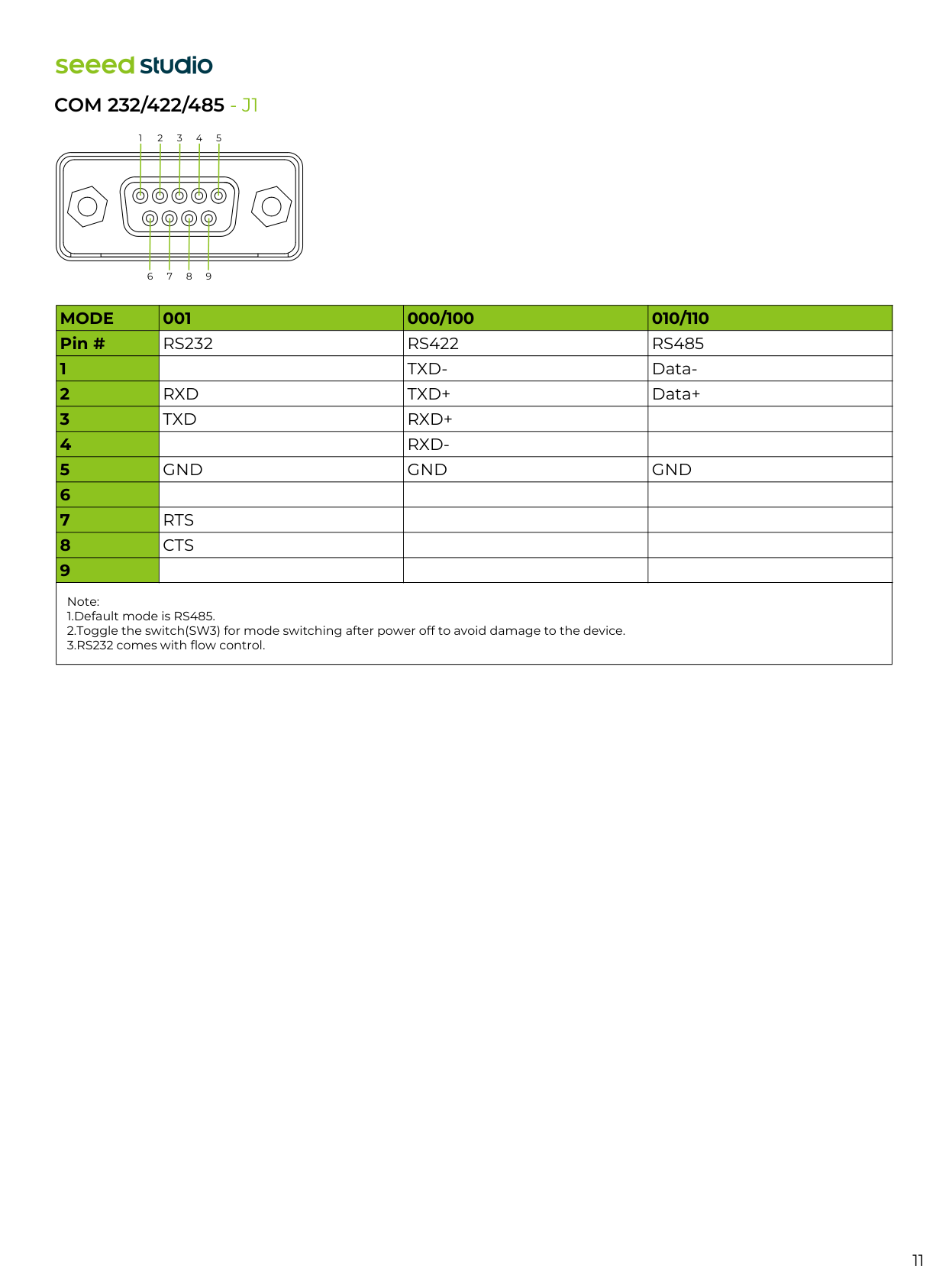
Com 232/422/485 - J1
1 2 3 4 5 6 7 8 9 Note: 1.Default mode is RS485. 2.Toggle the switch(SW3) for mode switching after power off to avoid damage to the device. 3.RS232 comes with flow control.Mode
001 000/100 010/110 Pin # 1 2 3 4 5 6 7 8 9Rs232
Rs422
Rs485
Txd-
Data-Rxd
Txd+
Data+Txd
Rxd+
Rxd-
Gnd
Gnd
Gnd
Rts
Cts
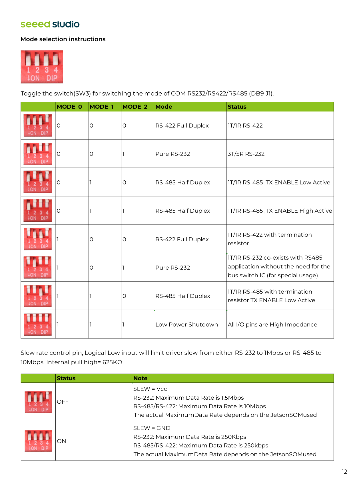
12 Slew rate control pin, Logical Low input will limit driver slew from either RS-232 to 1Mbps or RS-485 to 10Mbps. Internal pull high= 625KΩ. Status Note
Off
On
SLEW = Vcc RS-232: Maximum Data Rate is 1.5Mbps RS-485/RS-422: Maximum Data Rate is 10Mbps The actual MaximumData Rate depends on the JetsonSOMusedSlew = Gnd
RS-232: Maximum Data Rate is 250Kbps RS-485/RS-422: Maximum Data Rate is 250kbps The actual MaximumData Rate depends on the JetsonSOMused Mode selection instructions Toggle the switch(SW3) for switching the mode of COM RS232/RS422/RS485 (DB9 J1).Mode_0
Mode_1
Mode_2
Mode Status 0 0 0 RS-422 Full Duplex1T/1R Rs-422
0 0 1 Pure RS-2323T/5R Rs-232
0 1 0 RS-485 Half Duplex 1T/1R RS-485 ,TX ENABLE Low Active 0 1 1 RS-485 Half Duplex 1T/1R RS-485 ,TX ENABLE High Active 1 0 0 RS-422 Full Duplex 1T/1R RS-422 with termination resistor 1 0 1 Pure RS-232 1T/1R RS-232 co-exists with RS485 application without the need for the bus switch IC (for special usage). 1 1 0 RS-485 Half Duplex 1T/1R RS-485 with termination resistor TX ENABLE Low Active 1 1 1 Low Power Shutdown All I/O pins are High Impedance
13 Note:
Dp1_Txd0 (Hdmi_Txd2)_P
65Hdmi_Txd2_Con_P
HDMI Transmit Data 2+ Output – – Ground GroundDp1_Txd0 (Hdmi_Txd2)_N
63Hdmi_Txd2_ Con_N
HDMI Transmit Data 2– OutputDp1_Txd1 (Hdmi_Txd1)_P
71Hdmi_Txd1_ Con_P
HDMI Transmit Data 1+ Output – – Ground GroundDp1_Txd1 (Hdmi_Txd1)_N
69Hdmi_Txd1_ Con_N
HDMI Transmit Data 1– OutputDp1_Txd2 (Hdmi_Txd0)_P
77Hdmi_Txd0_ Con_P
HDMI Transmit Data 0+ Output – – Ground GroundDp1_Txd2 (Hdmi_Txd0)_N
75Hdmi_Txd0_ Con_N
HDMI Transmit Data 0– OutputDp1_Txd3 (Hdmi_Txc)_P
83Hdmi_Txc_Con_P
HDMI Transmit Clock+ Output – – Ground GroundDp1_Txd3 (Hdmi_Txc)_N
81Hdmi_Txc_Con_N
HDMI Transmit Clock– OutputHdmi_Cec
94Hdmi_Cec
Hdmi Cec
Bidir – – Unused UnusedDp1_Aux_P (Hdmi_Ddc_Scl)
100Hdmi_Ddc_Scl_5V0
HDMI DDC Clock Output /ODDp1_Aux_N (Hdmi_Ddc_Sda) 98
HDMI_DDC_SDA_5V0 HDMI DDC Data Bidir/OD – – Ground Ground – –Vdd_5V0_Hdmi_Co
HDMI 5V Power PowerDp1_Hpd (Hdmi_Hpd)
96Hdmi_Hpd_Con
HDMI Hot Plug Detect Input
14 USB3.1 TYPE-A x2 - J3 Note:
Usb1_D_N
115Usb2_A_N
USB 2.0 #3 Data from hub BidirUsb1_D_P
117Usb2_A_P
– – Ground GroundUsbss_Rx_N
161Usbss_Rx_A_Con2_N
USB 3.1 Receive Data from hub InputUsbss_Rx_P
163Usbss_Rx_A_Con2_P
– – Ground GroundUsbss_Tx_N
166Usbss_Tx_A_Con2_N
USB 3.1 Transmit Data from hub OutputUsbss_Tx_P
168Usbss_Tx_A_Con2_P
– – – VBUS Supply PowerUsb1_D_N
115Usb1_A_N
USB 2.0 #3 Data from hub BidirUsb1_D_P
117Usb1_A_P
– – Ground GroundUsbss_Rx_N
161Usbss_Rx_A_Con1_N
USB 3.1 Receive Data from hub InputUsbss_Rx_P
163Usbss_Rx_A_Con1_P
– – Ground GroundUsbss_Tx_N
166Usbss_Tx_A_Con1_N
USB 3.1 Transmit Data from hub OutputUsbss_Tx_P
168Usbss_Tx_A_Con1_P
15 Reset button: the reset button executes a hard reset on the system. USB3.1 TYPE-A x2 - J4 RESET Button Note:
Usb1_D_N
115Usb2_A_N
USB 2.0 #3 Data from hub BidirUsb1_D_P
117Usb2_A_P
– – Ground GroundUsbss_Rx_N
161Usbss_Rx_A_Con2_N
USB 3.1 Receive Data from hub InputUsbss_Rx_P
163Usbss_Rx_A_Con2_P
– – Ground GroundUsbss_Tx_N
166Usbss_Tx_A_Con2_N
USB 3.1 Transmit Data from hub OutputUsbss_Tx_P
168Usbss_Tx_A_Con2_P
– – – VBUS Supply PowerUsb1_D_N
115Usb1_A_N
USB 2.0 #3 Data from hub BidirUsb1_D_P
117Usb1_A_P
– – Ground GroundUsbss_Rx_N
161Usbss_Rx_A_Con1_N
USB 3.1 Receive Data from hub InputUsbss_Rx_P
163Usbss_Rx_A_Con1_P
– – Ground GroundUsbss_Tx_N
166Usbss_Tx_A_Con1_N
USB 3.1 Transmit Data from hub OutputUsbss_Tx_P
168Usbss_Tx_A_Con1_P
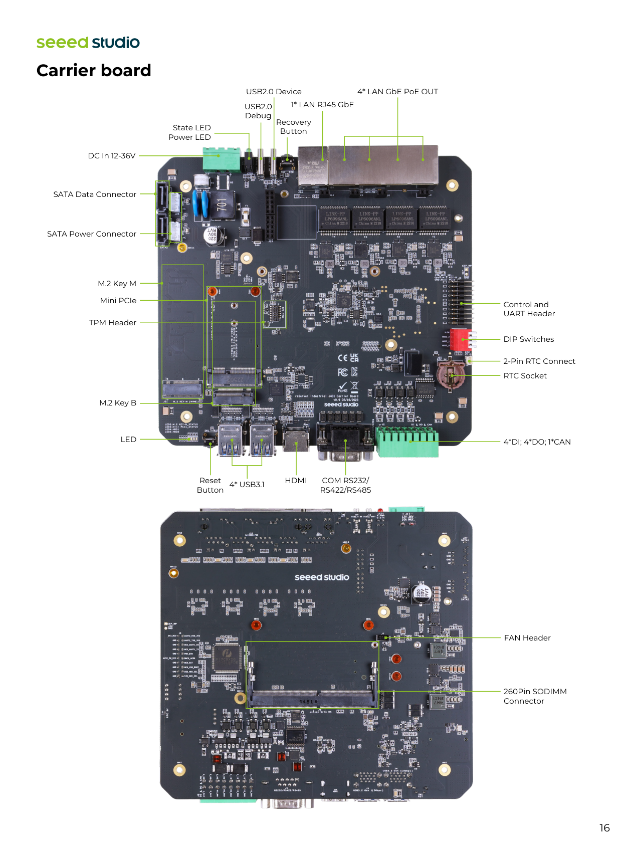
16 DIP Switches Control and UART Header 2-Pin RTC Connect RTC Socket
4*Di; 4*Do; 1*Can
4* LAN GbE PoE OUT 1* LAN RJ45 GbE USB2.0 DeviceUsb2.0
Debug State LED Power LED DC In 12-36V SATA Data Connector SATA Power Connector Recovery Button Carrier board M.2 Key M Mini PCIe M.2 Key BLed
TPM Header 260Pin SODIMM Connector FAN Header4* Usb3.1
Hdmi
Com Rs232/
Rs422/Rs485
Reset Button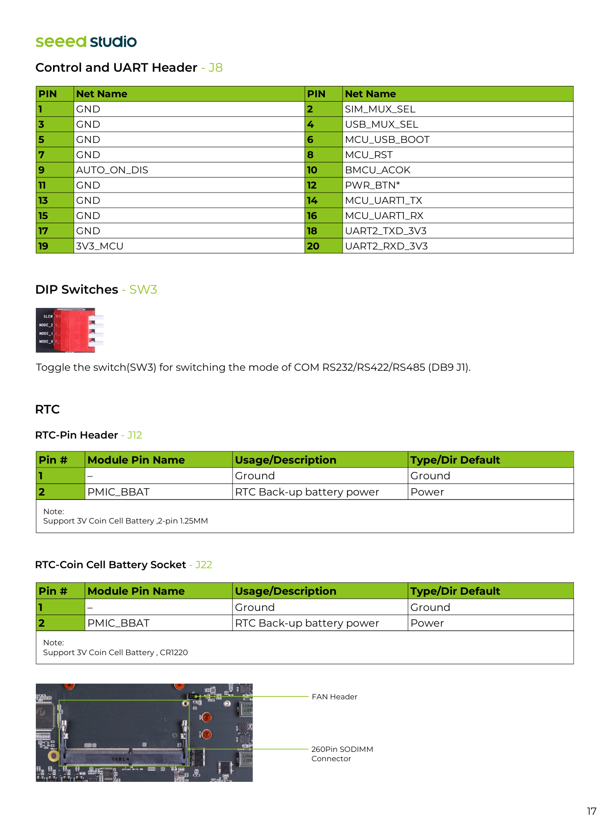
DIP Switches - SW3 RTC-Pin Header - J12 RTC-Coin Cell Battery Socket - J22
Rtc
17 Toggle the switch(SW3) for switching the mode of COM RS232/RS422/RS485 (DB9 J1). Note: Support 3V Coin Cell Battery ,2-pin 1.25MM Note: Support 3V Coin Cell Battery , CR1220 260Pin SODIMM Connector FAN Header Pin # Module Pin Name Usage/Description Type/Dir Default 1 2 – Ground GroundPmic_Bbat
RTC Back-up battery power Power Pin # Module Pin Name Usage/Description Type/Dir Default 1 2 – Ground GroundPmic_Bbat
RTC Back-up battery power Power Control and UART Header - J8Pin
Net NamePin
Net Name 1 2 3 4 5 6 7 8 9 10 11 12 13 14 15 16 17 18 19 20Gnd
Sim_Mux_Sel
Gnd
Usb_Mux_Sel
Gnd
Mcu_Usb_Boot
Gnd
Mcu_Rst
Auto_On_Dis
Bmcu_Acok
Gnd
Pwr_Btn*
Gnd
Mcu_Uart1_Tx
Gnd
Mcu_Uart1_Rx
Gnd
Uart2_Txd_3V3
3V3_Mcu
Uart2_Rxd_3V3
18
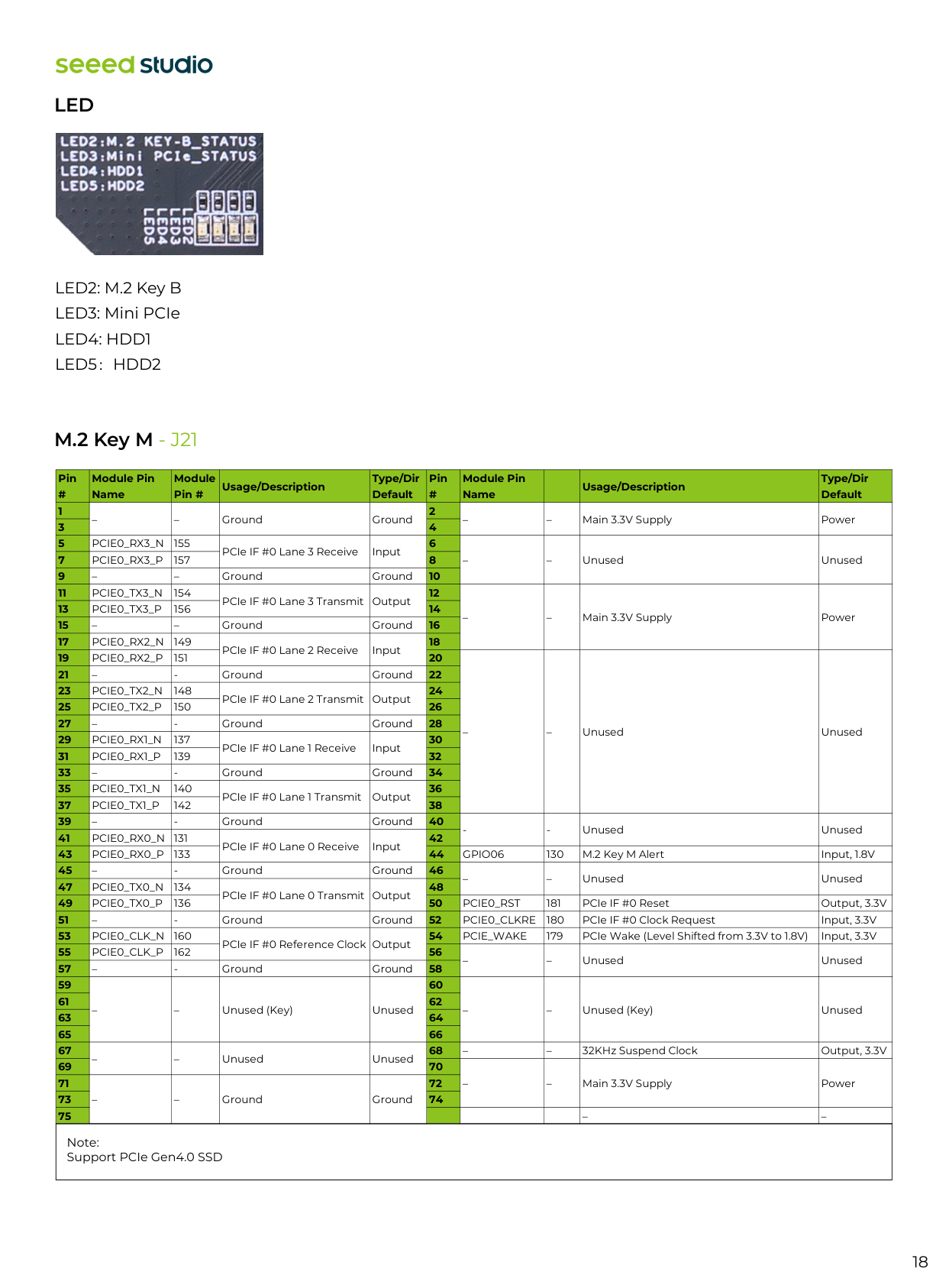
Led
M.2 Key M - J21 LED2: M.2 Key B LED3: Mini PCIeLed4: Hdd1
Led5:Hdd2
Note: Support PCIe Gen4.0 SSD – – Ground Ground – – Main 3.3V Supply PowerPcie0_Rx3_N
155 PCIe IF #0 Lane 3 Receive Input – – Unused UnusedPcie0_Rx3_P
157 – – Ground GroundPcie0_Tx3_N
154 PCIe IF #0 Lane 3 Transmit Output – – Main 3.3V Supply PowerPcie0_Tx3_P
156 – – Ground GroundPcie0_Rx2_N
149 PCIe IF #0 Lane 2 Receive InputPcie0_Rx2_P
151 – – Unused Unused –Pcie0_Tx2_N
148 PCIe IF #0 Lane 2 Transmit OutputPcie0_Tx2_P
150 –Pcie0_Rx1_N
137 PCIe IF #0 Lane 1 Receive InputPcie0_Rx1_P
139 –Pcie0_Tx1_N
140 PCIe IF #0 Lane 1 Transmit OutputPcie0_Tx1_P
142 –Pcie0_Rx0_N
131 PCIe IF #0 Lane 0 Receive InputPcie0_Rx0_P
133Gpio06
130 M.2 Key M Alert Input, 1.8V –Pcie0_Tx0_N
134 PCIe IF #0 Lane 0 Transmit OutputPcie0_Tx0_P
136Pcie0_Rst
181 PCIe IF #0 Reset Output, 3.3V –Pcie0_Clkre
180 PCIe IF #0 Clock Request Input, 3.3VPcie0_Clk_N
160 PCIe IF #0 Reference Clock OutputPcie_Wake
179 PCIe Wake (Level Shifted Pin # Module Pin Name Module Pin # Usage/Description Type/Dir Default Pin # Module Pin Name Usage/Description Type/Dir Default 1 2 3 4 5 6 7 8 9 10 11 12 13 14 15 16 17 18 19 20 21 22 23 24 25 26 27 28 29 30 31 32 33 34 35 36 37 38 39 40 41 42 43 44 45 46 47 48 49 50 51 52 53 54 55 56 57 58 59 60 61 62 63 64 65 66 67 68 69 70 71 72 73 74 75 from 3.3V to 1.8V) Input, 3.3VPcie0_Clk_P
162 – – Unused Unused –
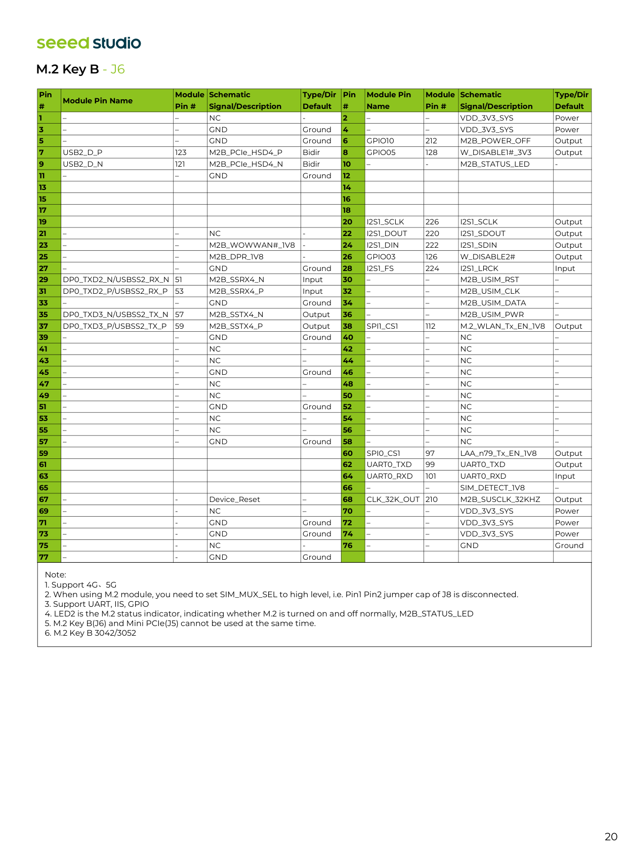
TPM Header - J11 19 Note: Support SPI interface TPM module, test with TPM2.0 Module with infineon SLB9670 (module not included) Mini PCIe - J5 Note: 1.Support 4G/LoRaWAN®/GPS. 2.When using Mini PCIe 4G module, you need to set SIM_MUX_SEL to low level (Pin1 Pin2 jumper cap of J8 is connected), when using LoRa module, you need to disconnect SIM card signal, at this time you need to set SIM_MUX_SEL to high level(Pin1 Pin2 jumper cap of J8 is disconnected). 3.Can be used as UART, IIC, GPIO. 4.M.2 Key B(J6) and Mini PCIe(J5) cannot be used at the same time. Pin # Module Pin Name Module Pin # Schematic Signal/Description Type/Dir Default Pin # Module Pin Name Module Pin # Schematic Signal/Description Type/Dir Default 1 2 3 4 5 6 7 8 9 10 11 12 13 14 15 16 17 18 19 20 21 22 23 24 25 26 27 28 29 30 31 32 33 34 35 36 37 38 39 40 41 42 43 44 45 46 47 48 49 50 51 52 – – PCIe_WAKE_3V3 #I2C Expansion IO-GPIO304 – – –
Vdd_3V3_Sys
Power – –Nc
– – –Gnd
Ground – –Nc
– – –Nc
– – –Nc
– – – PCIe_USIM_PWR – – –Gnd
Ground – – PCIe_USIM_DATA –Uart0_Txd
99Uart0_Txd_3V3
Output – – PCIe_USIM_CLK –Uart0_Rxd 101
Uart0_Rxd_3V3
Input – – PCIe_USIM_RST – – –Gnd
Ground – –Nc
– – –Nc
– – –Gnd
GroundGpio05
128W_Disable1#_3V3
Output – –Gnd
GroundUart0_Rts
Uart0_Rts_3V3
Output – –Vdd_3V3_Sys
PowerUart0_Cts
105Uart0_Cts_3V3
Input – –Gnd
Ground – –Gnd
Ground – –Nc
– – –Gnd
GroundI2C1_Scl
189I2C1_Scl
OutputI2C1_Sda
191I2C1_Sda
Bidir – –Nc
– – –Gnd
Ground – –Gnd
GroundUsb2_D_N
121 M2B_PCIe_HSD4_N Bidir – –Gnd
GroundUsb2_D_P
123 M2B_PCIe_HSD4_P Bidir – –Vdd_3V3_Sys
Power – –Gnd
Ground – –Vdd_3V3_Sys
Power – –Led_Wwan
– – –Gnd
Ground – –Nc
–Spi1_Sck
106Spi1_Sck_3V3
Output – –Nc
–Spi1_Miso
108Spi1_Miso_3V3
Input – –Nc
–Spi1_Mosi
104Spi1_Mosi_3V3
Output – –Gnd
GroundSpi1_Cs0
110Spi1_Cs0_3V3
Input – –Vdd_3V3_Sys
PowerPin
Schematic SignalPin
Schematic Signal 1 2 3 4 5 6 7 8 9 10 11 12 13 14Vdd_Tpm
Spi0_Irq_Ls
Spi0_Rst_Ls
Nc
Nc
Nc
Vdd_Tpm
Gnd
Spi0_Cs0_Ls
Spi0_Sck_Ls
Spi0_Miso_Ls
Pi0_Mosi_Ls
Nc
Nc
Note:
Nc
Vdd_3V3_Sys
Power – –Gnd
Ground – –Vdd_3V3_Sys
Power – –Gnd
GroundGpio10
212M2B_Power_Off
OutputUsb2_D_P
123 M2B_PCIe_HSD4_P BidirGpio05
128W_Disable1#_3V3
OutputUsb2_D_N
121 M2B_PCIe_HSD4_N Bidir –M2B_Status_Led
Gnd
GroundI2S1_Sclk
226I2S1_Sclk
Output – –Nc
I2S1_Dout
I2S1_Sdout
Output – –M2B_Wowwan#_1V8
I2S1_Din
I2S1_Sdin
Output – –M2B_Dpr_1V8
Gpio03
W_Disable2#
Output – –Gnd
GroundI2S1_Fs
224I2S1_Lrck
InputDp0_Txd2_N/Usbss2_Rx_N 51
M2B_Ssrx4_N
Input – –M2B_Usim_Rst
–Dp0_Txd2_P/Usbss2_Rx_P
53M2B_Ssrx4_P
Input – –M2B_Usim_Clk
– – –Gnd
Ground – –M2B_Usim_Data
–Dp0_Txd3_N/Usbss2_Tx_N
57M2B_Sstx4_N
Output – –M2B_Usim_Pwr
–Dp0_Txd3_P/Usbss2_Tx_P
59M2B_Sstx4_P
OutputSpi1_Cs1
112 M.2_WLAN_Tx_EN_1V8 Output – –Gnd
Ground – –Nc
– – –Nc
– – –Nc
– – –Nc
– – –Nc
– – –Gnd
Ground – –Nc
– – –Nc
– – –Nc
– – –Nc
– – –Nc
– – –Gnd
Ground – –Nc
– – –Nc
– – –Nc
– – –Nc
– – –Nc
– – –Gnd
Ground – –Nc
–Spi0_Cs1
97 LAA_n79_Tx_EN_1V8 OutputUart0_Txd
99Uart0_Txd
OutputUart0_Rxd
101Uart0_Rxd
Input – –Sim_Detect_1V8
– –Clk_32K_Out 210
M2B_Susclk_32Khz
Output –Nc
Vdd_3V3_Sys
Power –Gnd
Vdd_3V3_Sys
Power –Gnd
Vdd_3V3_Sys
Power –Nc
Gnd
Ground Pin # Module Pin Name Module Pin # Schematic Signal/Description Type/Dir Default Pin # Module Pin Name Module Pin # Schematic Signal/Description Type/Dir Default 1 2 3 4 5 6 7 8 9 10 11 12 13 14 15 16 17 18 19 20 21 22 23 24 25 26 27 28 29 30 31 32 33 34 35 36 37 38 39 40 41 42 43 44 45 46 47 48 49 50 51 52 53 54 55 56 57 58 59 60 61 62 63 64 65 66 67 68 69 70 71 72 73 74 75 76 77 –Gnd
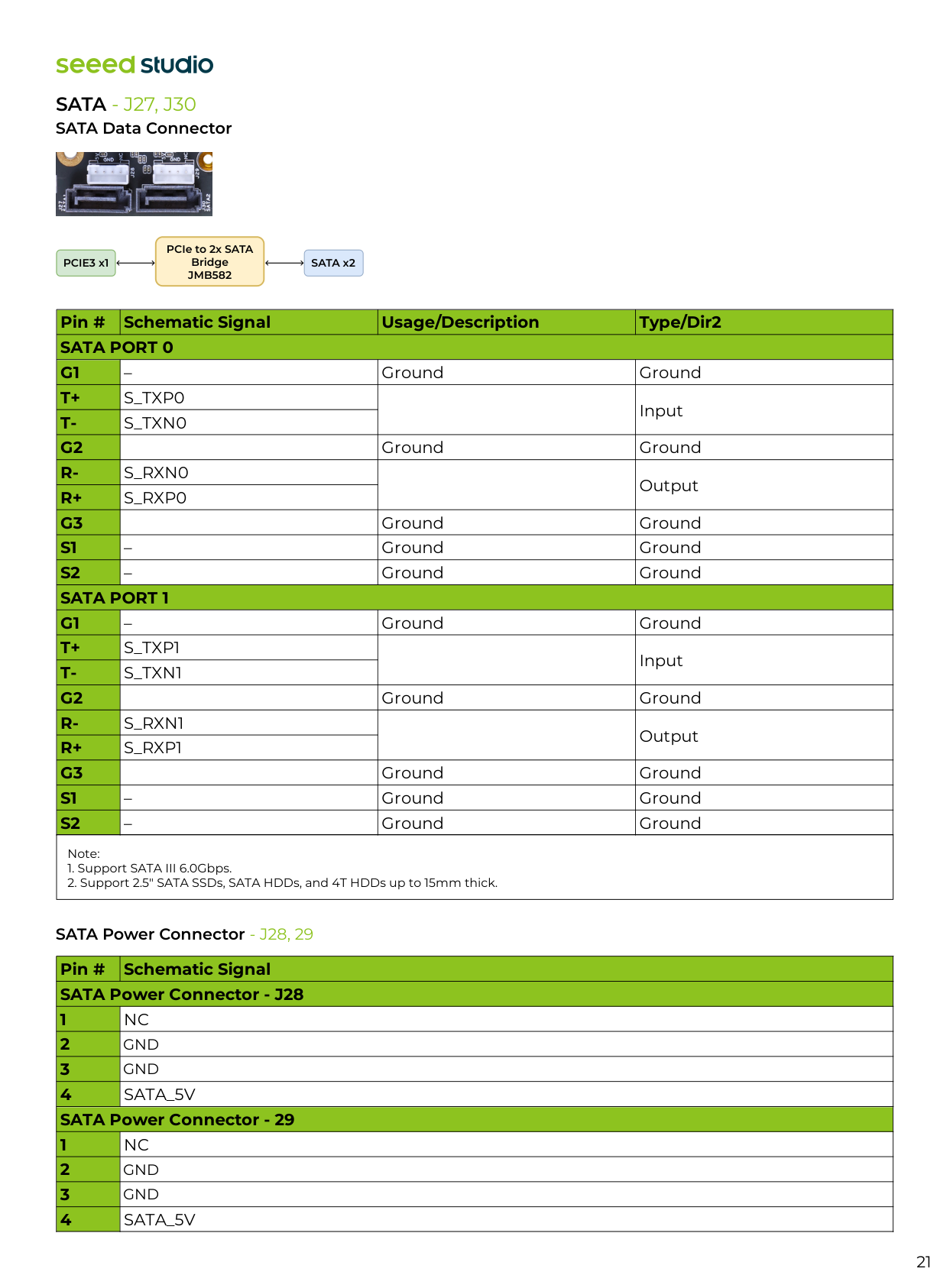
21 SATA Data Connector
Sata - J27, J30
SATA Power Connector - J28, 29 Note:Jmb582
Pin # Schematic Signal Usage/Description Type/Dir2Sata Port 0
G1
T+
T-
G2
R-
R+
G3
S1
S2
Sata Port 1
G1
T+
T-
G2
R-
R+
G3
S1
S2
– Ground GroundS_Txp0
InputS_Txn0
Ground GroundS_Rxn0
OutputS_Rxp0
Ground Ground – Ground Ground – Ground Ground – Ground GroundS_Txp1
InputS_Txn1
Ground GroundS_Rxn1
OutputS_Rxp1
Ground Ground – Ground Ground – Ground Ground Pin # Schematic Signal SATA Power Connector - J28 1 2 3 4 SATA Power Connector - 29 1 2 3 4Nc
Sata_5V
Nc
Sata_5V
Gnd
Gnd
Gnd
Gnd
22 Dimensions Accessories Information Please kindly know that the accessories below are not included in the package. We provide the information here to help you choose the appropriate accessories. Pre-installed Jetpack 5.1.1 (above) (provide Linux OS with board support package). reServer Industrial comes with M.2 NVMe 2280 SSD 128G with OS pre-installed in the SSD. If you need to reflash the image, please refer to our wiki for details. Pre-installed OS Type Product Name
Gps
4G
5G
LoRaWANTpm
Ec25Euxga-Minipcie;
Ec25Euxga-Minipcie; Ec20Cehclg-Minipcie
Sim8202G-M2
Wio-WM1302 LoRaWAN Gateway Module (SPI) - US915 - M TPM2.0 module with Infineon SLB9670 Unit: mm 180.00mm 194.33mm 75.00mm 15.00mm 100.00mm 75.00mm 100.00mm 187.00mm 194.61mm 95.50mm 98.00mm FAN Header -J7 Note: 1.Whether the fan is self-starting or starts only when it reaches the temperature can be set by yourself. 2.Connect 4Pin 5V fan, fan speed can be controlled, and the speed can be detected. Pin # Module Pin Name Module Pin # Schematic Signal 1 2 3 4 – – – –Gpio08 (Sdmmc_Cd)
208Fan_Tach
Gpio14 (Pwm)
230Fan_Pwm
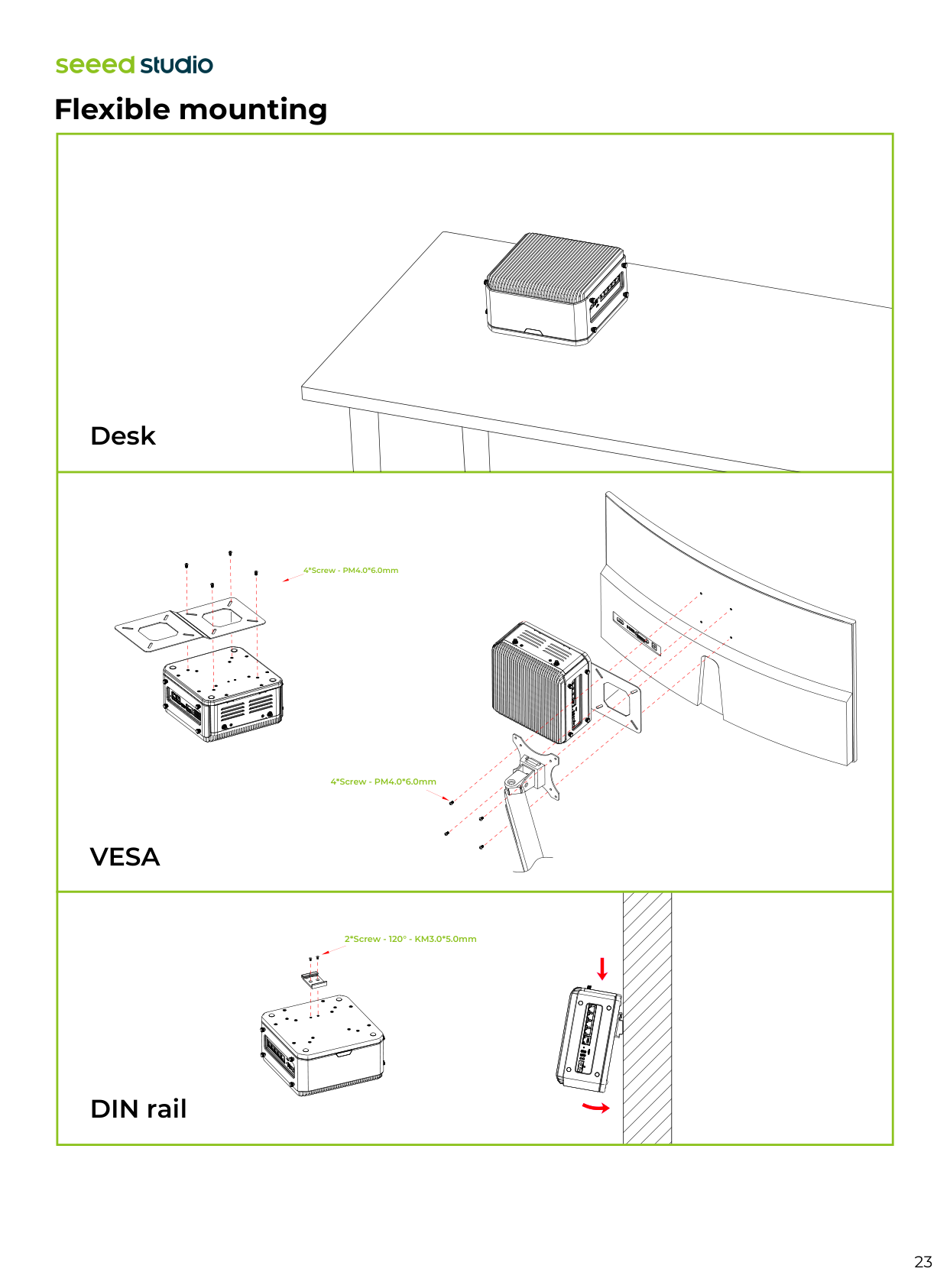
23 Flexible mounting
Vesa
DIN rail Desk 4*Screw - PM4.0*6.0mm 4*Screw - PM4.0*6.0mm 2*Screw - 120° - KM3.0*5.0mm
24 More information Please check our wiki to learn more about this device and if you have any questions, feel free to reach out to our Forum and Discord community. For more information, you can also refer to NVIDIA official Jetson Download Center Scan for more information Forum Discord Wiki Certifications